
 Deutsch
Chemical surface treatment, etching and cleaning of silicon and other materials
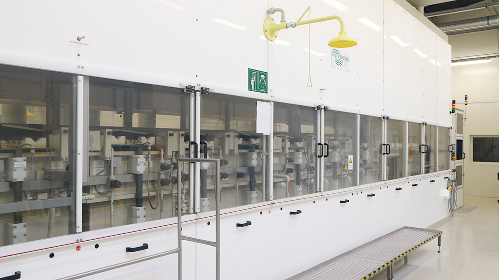
Silicon etching: We have fully and partially automated etching equipment that can chemically treat materials of varying sizes and morphologies. The surface cleaning or the removing of layers takes place in batch processes or continuously operating lines.
- For photovoltaic applications: Chemical surface treatment and cleaning of silicon materials across the entire photovoltaic value chain: from coarse material to fine silicon (from 50 μm)
- For photovoltaic and semiconductor industry: Polish etching of seed crystals, cleaning cell trays, wafer carriers or boats from CVD tools (silicon nitride), selective removal of metals or metallic impurities
- Recovery of valuable materials: Selective etching of metals and compound semiconductors and recovery of valuable materials (precipitation, electrolysis, etc.)